
PCB Depaneling Machines
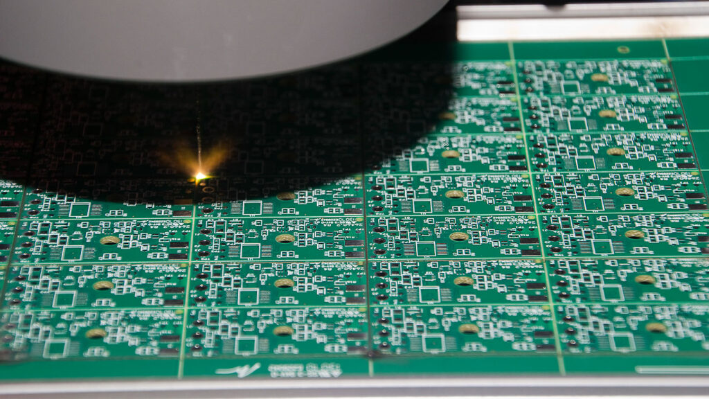
Laser cutting of PCBs is a common method for separating smaller circuits from a larger board array. Replace traditional mechanical routing techniques with a non-contact, high-precision laser depaneling system.
System Overview
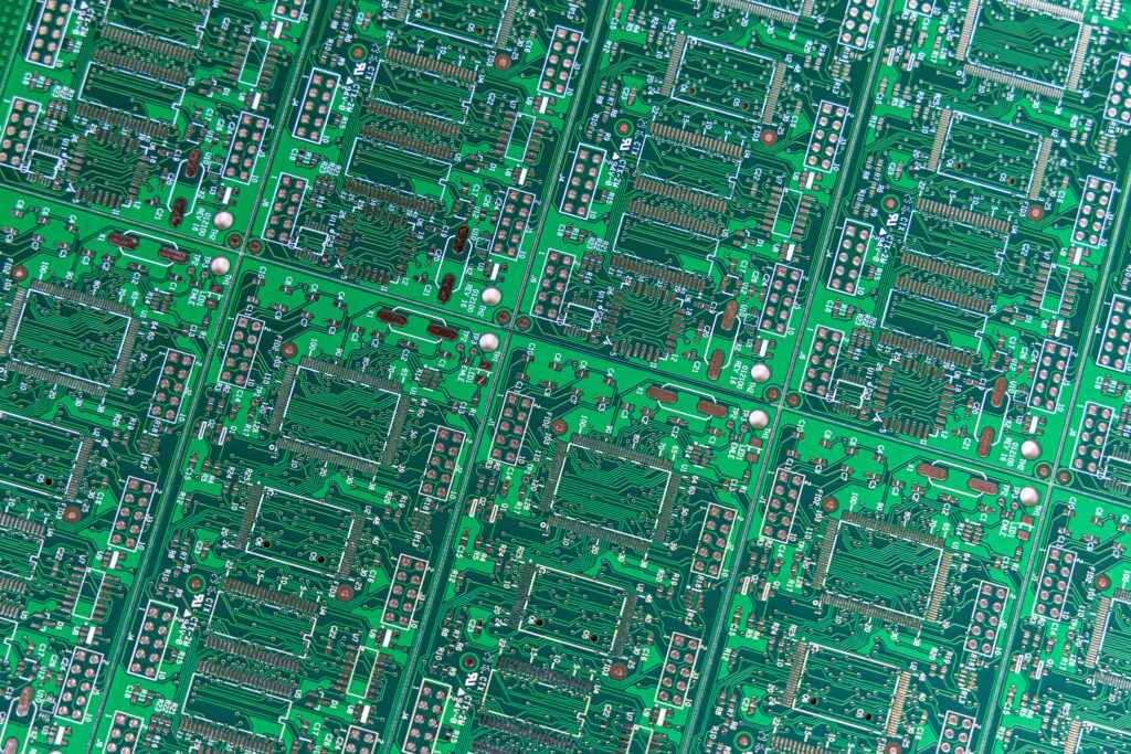
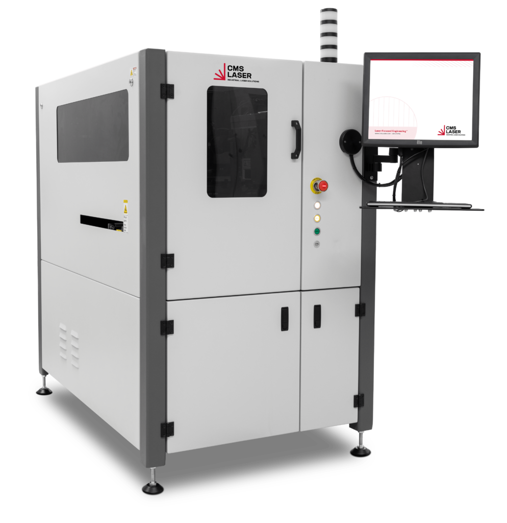
Laser depaneling systems are gaining popularity—especially as circuit board complexity and component ratios continue to rise. Our standard UV and CO2 depaneling systems configuration features machine vision for locating board fiducials to cut PCBs with pinpoint accuracy. Cut rigid and flex boards using a non-contact method, while achieving close tolerances and minimal debris.

- Laser cutting source with machine vision for locating board fiducial markings
- CO2 or UV laser sources available—based on applications lab testing results
- PCB conveyor capable of carrying boards up to 20″ x 18″ in size
- Automatic board entrance/exit slots with safety interlocks
- Systems configured for standalone operation or SMT line integration
- Welded steel frame with aluminum paneling for long-lasting industrial use
- CDRH Class 1 laser workstation with emergency stop push button
- Ergonomic arm with 19” monitor, keyboard, and mouse or touchscreen display
- CMS LaserGraf5 software with Windows® 10 64-bit operating system

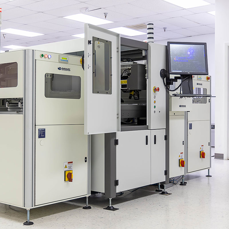
Standalone PCB Depaneler:
- CDRH Class 1 tower workstation enclosure
- Fiber (IR), CO2, UV, or Green laser sources available
- XY Table for fixtures
- Through the optics vision (TTOV) for locating fiducials
Conveyor Type System:
- CDRH Class 1 laser system with laser safety windows
- XY gantry laser source for PCB conveyor configuration
- Automatic board entry and exit doors
- Conveyor based system – 39.38in (1000mm) x 63.50in (1613mm) x 63.50in (1588mm)
CMS Laser PCB Depaneling Systems
Models Available


*Overall system design and size will vary based on customer requirements and applications lab testing results prior to purchase
PCB Cutting Laser Technology
High-precision laser cutting for printed circuit boards
Depaneling Circuit Boards
Separate printed circuit board arrays using a CO2 or UV laser. This method produces zero mechanical stress on the board and surrounding components.
- Non-contact laser cutting
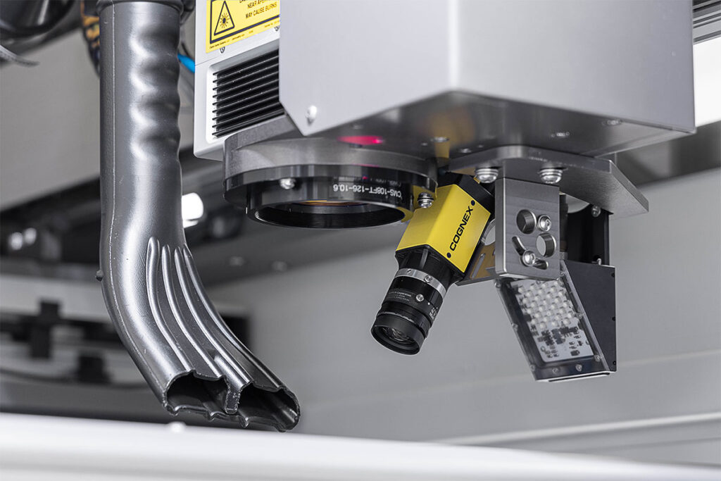
Machine Vision
Off-axis camera systems recognize board fiducials for aligning the laser cutting path. This ensures every cut is precisely where it needs to be.
- Precise repeatable results
In-line or Standalone Operation
Our engineers can design a system that meets your manufacturing goals. Whether you need an in-line conveyor or robot integration, we’ll build the system.
- Board stackers and de-stackers for standalone
- Integrate directly into SMT lines
Other Systems
PCB Marking Systems
Learn More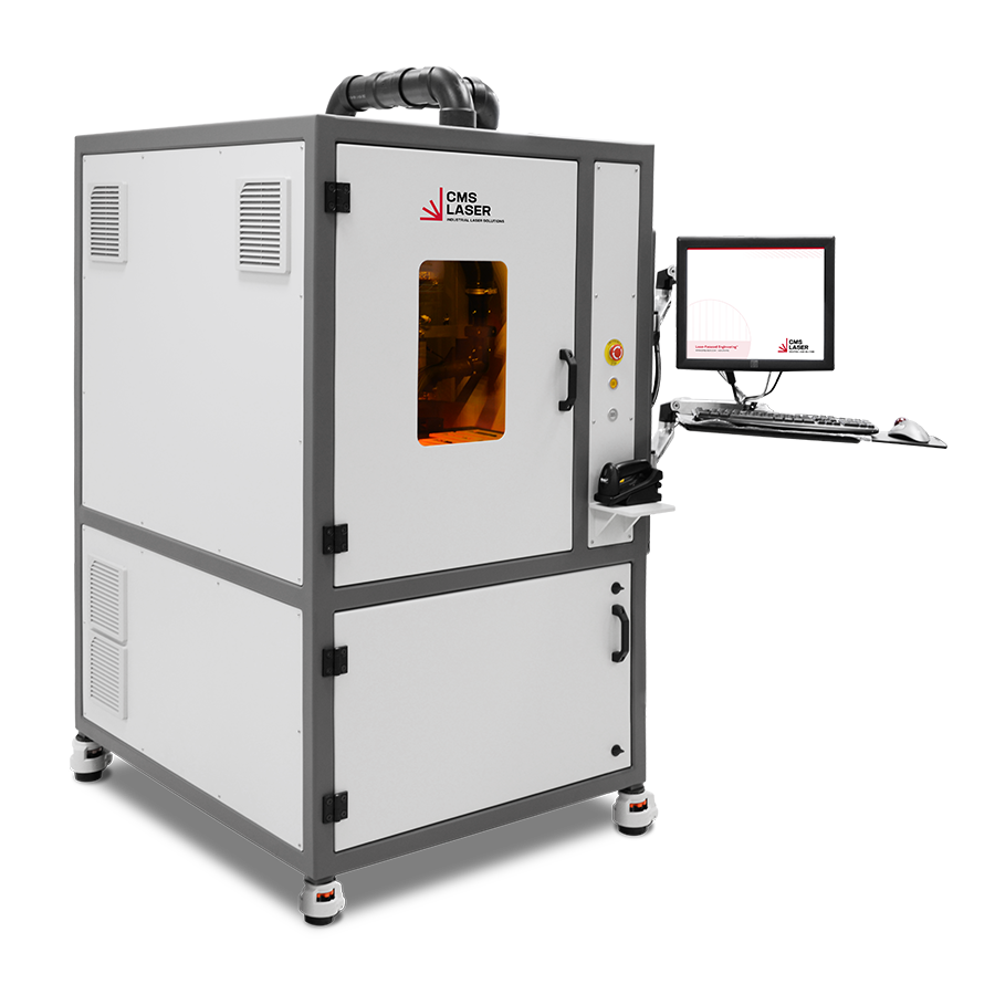
UV Laser Cutting for PCBs
Learn MoreThe Absolute Best Customer Service Around
Working with Control Micro Systems has been very easy. They have been attentive to our needs and worked to help us tremendously with our older model machine and new machines. We are pleased with the performance of their machines.
Working with the entire Control Micro Systems team on our project was a pleasure. CMS was capable of meeting and exceeding our goals. They successfully designed and built a machine which increased our throughput by 550%! We are so glad we chose to move forward with CMS.
CMS have been excellent partners in the development of new, complex equipment for our business. CMS built multiple machines for us. Each machine had a different purpose, however the CMS team worked openly & honestly with us to agree on optimal solutions for each one.
Struggling to Find the Right Solution?
Our USA-based experts are here to help!